

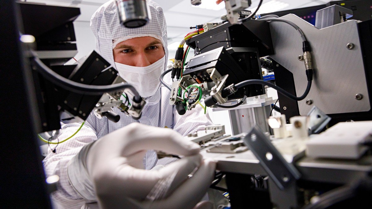
Samsung Electronics pulled back the curtain on its next-generation semiconductor roadmap on September 22, 2026, during the Samsung Foundry Forum held in Seoul. Addressing hundreds of fabless chip designers, cloud hyperscalers, and global technology partners, the South Korean conglomerate unveiled a consolidated turnkey service model integrating 2-nanometer (nm) Gate-All-Around (GAA) fabrication with proprietary advanced packaging architectures.
The strategic core of Samsung's presentation was its all-in-one 'One-Stop AI Solution'. Unlike competitors who separate contract wafer manufacturing from outsourced semiconductor assembly and test (OSAT) providers, Samsung uniquely controls the complete triad: leading-edge foundry nodes, High Bandwidth Memory (HBM3E and HBM4), and complex 2.5D and 3D heterogeneous packaging.
Single-Point Turnkey Architecture for High-Performance AI Accelerators
Company executives demonstrated that coordinating foundry processing, memory procurement, and packaging under a single operational roof shortens the commercialization timeline of generative AI application-specific integrated circuits (ASICs) by approximately 20%. The workflow eliminates multi-party shipping delays, simplifies thermal testing, and improves overall fabrication yields.
On the silicon manufacturing side, Samsung confirmed that its 2nm process node (SF2) is on schedule for high-volume commercial production. Compared to previous-generation 3nm GAA designs, SF2 delivers a 12% improvement in operational performance, a 25% increase in power efficiency, and a 5% reduction in overall die area, while incorporating backside power delivery network (BSPDN) technology.
“By seamlessly uniting our leading-edge 2nm GAA foundry, world-class HBM memory, and innovative 3D packaging under a single turnkey roof, Samsung provides AI pioneers with an unmatched speed-to-market advantage.”
SAINT and I-Cube Packaging Technologies Drive Heterogeneous Integration
To connect massive AI processors with memory cubes, Samsung highlighted its SAINT (Samsung Advanced Interconnect Technology) platform. The company showcased SAINT-D, which vertically stacks HBM memory dies directly onto processor logic dies without micro-bumps, as well as the 2.5D I-CubeE interposer capable of integrating up to 12 HBM4 memory stacks alongside dual AI accelerator compute chiplets.
The showcase represents Samsung's aggressive bid to capture market share in high-margin AI accelerator and data-center chips, presenting a potent alternative to Taiwan Semiconductor Manufacturing Co. (TSMC). Supported by expanding cleanroom capacities across its Pyeongtaek complex and its new fab in Taylor, Texas, Samsung is positioning itself as the indispensable manufacturing engine of the global artificial intelligence boom.


Comments (0)
Log in to join the discussion.