

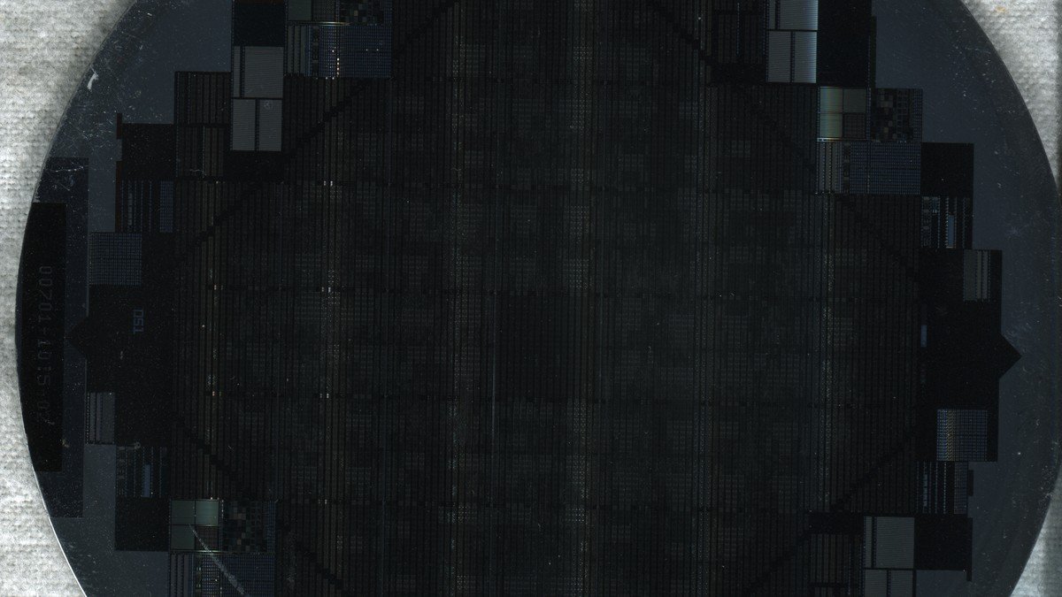
Tata Electronics has taken a landmark leap in realizing India's domestic semiconductor ambitions, signing a comprehensive strategic memorandum of understanding (MoU) with Japanese semiconductor equipment powerhouse Tokyo Electron Limited (TEL). The collaboration focuses on procuring advanced fabrication machinery and establishing workforce training pipelines for Tata's flagship ₹91,000 crore ($11 billion) wafer fabrication plant currently under construction in Dholera, Gujarat.
Under the terms of the agreement, Tokyo Electron will supply vital front-end semiconductor manufacturing equipment, covering critical stages such as chemical vapor deposition (CVD), plasma etching, photoresist coating, and wafer cleaning systems. In addition, TEL will establish dedicated field engineering centers and technical training facilities to upskill Indian engineers in operating complex nano-scale cleanroom tools.
Crucial Equipment Supply and Technological Collaboration
The Dholera fab, being developed by Tata Electronics in technical partnership with Taiwan's Powerchip Semiconductor Manufacturing Corporation (PSMC), represents India's first commercial-scale semiconductor foundry. The greenfield facility is engineered to produce mature node chips at 28-nanometer, 40-nanometer, and 55-nanometer thresholds, catering to exploding global demand.
When fully operational, the Dholera manufacturing complex will boast a production capacity of up to 50,000 wafer starts per month. The output will supply critical integrated circuits for electric vehicles, automotive electronics, telecommunications infrastructure, consumer gadgets, and edge artificial intelligence processors.
“Partnering with Tokyo Electron accelerates our journey toward establishing India's first commercial semiconductor manufacturing ecosystem, ensuring world-class process precision from day one.” — Randhir Thakur, CEO and Managing Director of Tata Electronics
Strategic Blueprint for India's Semiconductor Sovereignty
The partnership directly advances the Indian government's $10 billion India Semiconductor Mission (ISM), which provides up to 50% fiscal support for approved fabrication projects. By anchoring global equipment suppliers like Tokyo Electron on Indian soil, the country seeks to insulate its technology sector against geopolitical supply chain shocks.
Executives from Tokyo Electron underscored that establishing an enduring operational presence in Gujarat reflects Japan's strategic alignment with India in securing resilient supply networks. The first phase of tool installations at Dholera is scheduled for late 2025, paving the way for commercial chip rollouts by 2026.
Frequently Asked Questions
What is the total investment in the Tata Dholera semiconductor fab?
The facility represents an estimated investment of ₹91,000 crore (approximately $11 billion).
What role will Tokyo Electron play in the project?
Tokyo Electron will supply critical wafer fabrication equipment and provide training and engineering support for Indian personnel.

Comments (0)
Log in to join the discussion.