

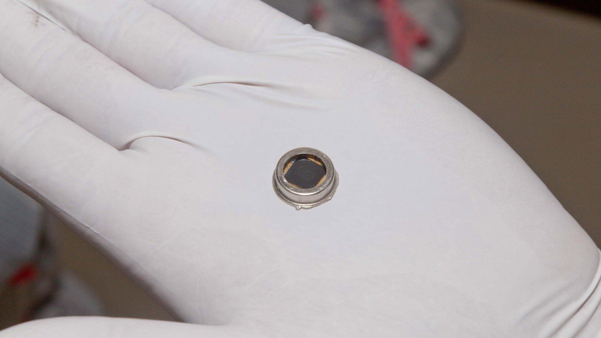
South Korean semiconductor heavyweight SK Hynix officially announced on Thursday that it has commenced the world's first commercial mass production of 12-layer High Bandwidth Memory (HBM3E) chips, achieving an industry-leading capacity of 36 gigabytes (GB). The milestone solidifies the company's commanding market lead in advanced artificial intelligence memory solutions and paves the way for volume customer deliveries starting before the end of the year.
The breakthrough 12-layer package increases memory capacity by 50 percent compared to previously dominant 8-layer, 24GB HBM3E modules, while maintaining the exact same physical package height. To accomplish this engineering feat, SK Hynix made each individual DRAM die 40 percent thinner than preceding generations and interconnected them vertically using advanced Through-Silicon Via (TSV) micro-pillar technology.
Next-Generation 36GB Memory Delivers Breakthrough Bandwidth for AI Models
Operating at unprecedented processing speeds of up to 9.6 gigabits per second, a single system configuration utilizing multiple 12-layer HBM3E stacks can transfer more than 1.22 terabytes of data per second—equivalent to transmitting 160 full-length high-definition movies in a single second. Such colossal throughput is vital for training and inferencing complex multimodal generative AI models.
SK Hynix confirmed that initial shipments will directly supply Nvidia for its forthcoming Blackwell Ultra B200 and GB200 NVL72 computing architectures. Nvidia currently commands over 85 percent of the global AI training accelerator market, making SK Hynix's primary supplier status a lucrative financial catalyst that propelled the memory maker to record quarterly operating profits.
“SK Hynix has once again broken technological barriers by becoming the first in the industry to mass-produce 12-layer HBM3E, cementing our uncontested leadership in AI memory.”
Proprietary Packaging Technology Widens Competitive Moat Over Rivals
To resolve the intense thermal challenges inherent in stacking twelve thin silicon dies into a micro-footprint, SK Hynix deployed its proprietary Advanced Mass Reflow Molded Underfill (MR-MUF) process. The specialized protective epoxy material enhances heat dissipation by 10 percent compared to competing thermo-compression bonding techniques, significantly improving reliability under continuous data center workloads.
The manufacturing breakthrough intensifies the competitive pressure on rival memory producers Samsung Electronics and Micron Technology, both of which are aggressively developing competing 12-layer HBM3E samples. However, with verified yields and finalized customer qualification already locked in, SK Hynix is positioned to capture the vast majority of premium tier AI memory demand through 2025.


Comments (0)
Log in to join the discussion.