

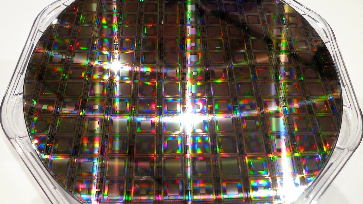
Memory powerhouse SK Hynix and contract foundry leader Taiwan Semiconductor Manufacturing Company (TSMC) announced a deepening of their strategic engineering alliance to co-develop sixth-generation High Bandwidth Memory, known as HBM4. The collaborative milestone marks a structural shift in how high-performance memory subsystems are designed and manufactured for massive artificial intelligence compute clusters.
Under the expanded framework, SK Hynix will integrate TSMC's advanced sub-3-nanometer logic processes directly onto the base die, or buffer die, at the foundation of each HBM4 stack. Previous generations of HBM utilized memory-optimized proprietary processes for base dies; shifting to TSMC's world-leading foundry logic allows designers to embed customized power routing, test circuitry, and specialized logic functions directly beneath the stacked DRAM layers.
Sub-3nm Base Dies Redefine Memory Logic Integration
This architectural evolution addresses the severe interconnect bottlenecks that threaten to constrain future generative AI accelerators. With memory bandwidth requirements surging alongside multi-trillion-parameter models, HBM4 doubles the interface bus width from 1,024 bits to 2,048 bits per stack, demanding unprecedented thermal efficiency and structural precision across micron-scale microbumps.
TSMC will also optimize its proprietary Chip-on-Wafer-on-Substrate (CoWoS) advanced packaging platforms to seamlessly interconnect SK Hynix's HBM4 modules with cutting-edge host processors, such as forthcoming architectures from Nvidia, AMD, and leading cloud service providers.
“Our collaboration with TSMC on HBM4 base dies ensures seamless performance integration, accelerating the development of customized AI memory for hyperscale customers.” — Justin Kim, President and Head of AI Infra at SK Hynix
CoWoS Packaging Synergy for Hyperscale AI Workloads
The joint development roadmap establishes a fortified competitive bulwark against rival integrated device manufacturers like Samsung Electronics and Micron Technology. By combining SK Hynix's preeminent position in commercial HBM3E supply with TSMC's undisputed packaging capacity and logic dominance, the duo aims to capture the lion's share of premium data center deployments through 2028.
Pilot tape-outs and qualification samples are slated to reach hyperscale technology partners by late 2025, paving the way for commercial volume manufacturing in the second half of 2026. Industry analysts predict the partnership will drastically compress deployment timelines for next-generation generative AI clusters worldwide.
Frequently Asked Questions
What is the primary technical breakthrough in the SK Hynix and TSMC HBM4 collaboration?
The alliance adopts TSMC's sub-3-nanometer foundry logic for the HBM4 base die, widening the interface bus to 2,048 bits and enabling customized on-chip logic directly beneath the memory stack.
When is commercial volume production of HBM4 memory expected?
Qualification samples will ship to major AI chipmakers in late 2025, with mass commercial production scheduled for the second half of 2026.


Comments (0)
Log in to join the discussion.