

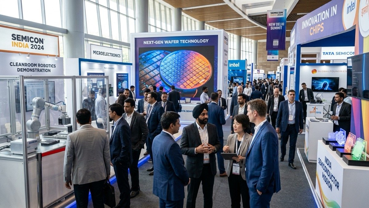
The premier microelectronics industry gathering in South Asia, SEMICON India 2026, inaugurated its three-day exhibition and policy conference today at the Bharat Mandapam in New Delhi. The event convenes senior executives from more than 600 semiconductor design, fabrication, chemicals, and precision lithography equipment companies, highlighting India's emergence as a strategic node in global silicon manufacturing diversification.
Inaugurating the summit, union leadership underscored the rapid implementation pace of the India Semiconductor Mission (ISM). Construction timelines across major fab projects in Gujarat and Assam were reported on schedule, with the initial assembly, testing, and packaging (ATMP) and outsourced semiconductor assembly and test (OSAT) facilities projected to commence commercial production within the next 14 months.
Commercial Milestones and Advanced Packaging Focus
Unlike previous summits centered primarily on financial pledges, this year's conference highlighted concrete engineering partnerships. Global equipment providers inked agreements with Indian industrial conglomerates to localize the supply of ultra-pure specialty gases, cleanroom chemical delivery infrastructure, and precision test sockets essential for operational fabs.
| Project Name / Location | Technology Node / Type | Estimated Investment | Operational Timeline |
|---|---|---|---|
| Dholera Commercial Fab (Gujarat) | 28nm / 40nm / 55nm Logic | $11.0 Billion | Commercial test runs late 2027 |
| Sanand Packaging Hub (Gujarat) | Advanced 2.5D / 3D OSAT | $2.75 Billion | Pilot production Q1 2027 |
| Morigaon ATMP Complex (Assam) | Automotive & Industrial Packaging | $3.2 Billion | Equipment fit-out mid 2027 |
| Sanand Compound Semi Unit | Silicon Carbide (SiC) Power Devices | $900 Million | Full-scale commissioning Q4 2026 |
Talent Development and University Integration
Addressing the chronic international shortage of semiconductor talent, the Ministry of Electronics and Information Technology (MeitY) unveiled an expanded VLSI design and fabrication curriculum. The initiative connects 120 premier technical universities with leading EDA (electronic design automation) software tools, guaranteeing subsidized access for over 85,000 engineering students annually.
International partners from Taiwan, Japan, and the United States commended India's collaborative strategy. Delegations pointed to rising geopolitical volatility in East Asian shipping corridors as a catalyst accelerating the need for secondary fabrication nodes in friendly Indo-Pacific democracies.
Strategic Road Ahead
Over the remaining sessions, delegates will debate the rollout of ISM 2.0, a secondary policy tranche anticipated to incentivize domestic manufacturing of semiconductor manufacturing equipment, compound gallium nitride (GaN) wafers, and advanced display glass panels.


Comments (0)
Log in to join the discussion.